 | –≠–ª–µ–∫—Ç—Ä–æ–Ω–Ω—ã–π –∫–æ–º–ø–æ–Ω–µ–Ω—Ç: LP2902N | –°–∫–∞—á–∞—Ç—å:  PDF PDF  ZIP ZIP |
LP2902/LP324
Micropower Quad Operational Amplifier
General Description
The LP324 series consists of four independent, high gain in-
ternally compensated micropower operational amplifiers.
These amplifiers are specially suited for operation in battery
systems while maintaining good input specifications, and ex-
tremely low supply current drain. In addition, the LP324 has
an input common mode range, and output source range
which includes ground, making it ideal in single supply appli-
cations.
These amplifiers are ideal in applications which include por-
table instrumentation, battery backup equipment, and other
circuits which require good DC performance and low supply
current.
Features
n
Low supply current:
125 µA (max)
n
Low offset voltage:
2 mV (max)
n
Low input bias current:
4 nA (max)
n
Input common mode to GND
n
Interfaces to CMOS logic
n
Wide supply range:
3V
<
V
+
<
32V
n
Small Outline Package available
n
Pin-for-pin compatible with LM324
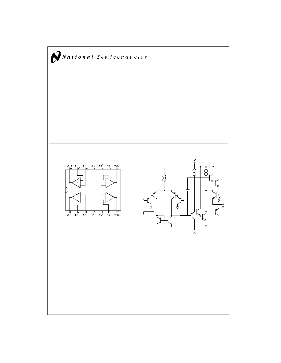
Connection Diagram
Simplified Schematic
Dual-In-Line (N) and SO (M)
DS008562-1
Order Number LP324M or LP2902M
See NS Package Number M14A
Order Number LP324N or LP2902N
See NS Package Number N14A
DS008562-2
September 1999
LP2902/LP324
Micropower
Quad
Operational
Amplifier
© 1999 National Semiconductor Corporation
DS008562
www.national.com
Absolute Maximum Ratings
(Note 1)
If Military/Aerospace specified devices are required,
please contact the National Semiconductor Sales Office/
Distributors for availability and specifications.
Supply Voltage
32V or
±
16V
LP2902
26V or
±
13V
Differential Input Voltage
32V
LP2902
26V
Input Voltage (Note 2)
-0.3V to 32V
LP2902
-0.3V to 26V
Output Short-Circuit to GND
Continuous
(One Amplifier) (Note 3)
V
+
15V and T
A
= 25∞C
ESD Susceptibility (Note 10)
±
500V
Operating Conditions
Package
N
M
Power Dissipation
500 mW
500 mW
(Note 4)
T
j
Max
150∞C
150∞C
ja
90∞C/W
140∞C/W
Operating Temp. Range
(Note 5)
(Note 5)
Storage Temp. Range
-65∞C
T
150∞C
Soldering
Information (10 sec.)
300∞C
260∞C
Vapor Phase (60 sec.)
215∞C
Infrared (15 sec.)
220∞C
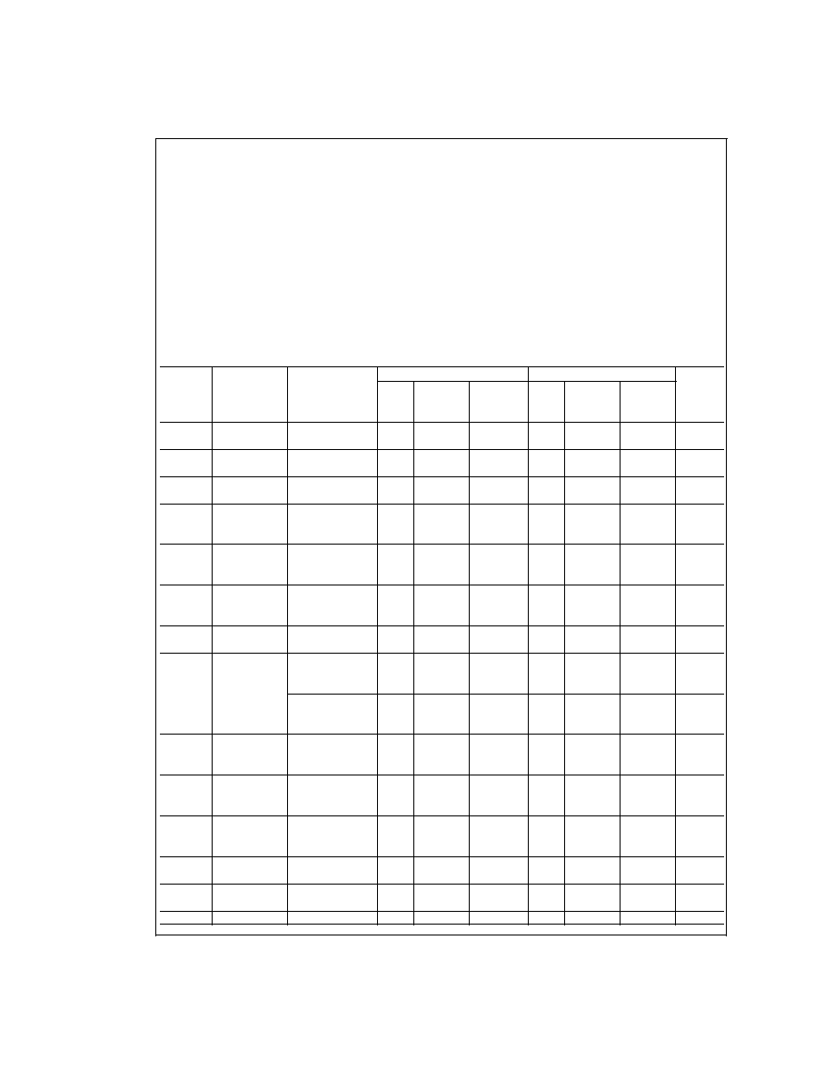
Electrical Characteristics
(Note 6)
LP2902 (Note 9)
LP324
Symbol
Parameter
Conditions
Tested
Design
Tested
Design
Units
Typ
Limit
Limit
Typ
Limit
Limit
Limits
(Note 7)
(Note 8)
(Note 7)
(Note 8)
V
os
Input Offset
2
4
10
2
4
9
mV
Voltage
(Max)
I
b
Input Bias
2
20
40
2
10
20
nA
Current
(Max)
I
os
Input Offset
0.5
4
8
0.2
2
4
nA
Current
(Max)
A
vol
Voltage
R
L
= 10k
70
40
30
100
50
40
V/mV
Gain
to GND
(Min)
V
+
= 30V
CMRR
Common
V
+
= 30V
90
80
75
90
80
75
dB
Mode Rej.
0V
V
cm
(Min)
Ratio
V
cm
<
V
+
- 1.5
PSRR
Power
V
+
= 5V to 30V
90
80
75
90
80
75
dB
Supply Rej.
(Min)
Ratio
I
s
Supply
R
L
=
85
150
250
85
150
250
µA
Current
(Max)
V
o
Output
I
L
= 350 µA
3.6
3.4
V
+
-1.9V
3.6
3.4
V
+
-1.9V
V
Voltage
to GND.
(Min)
Swing
V
cm
= 0V
I
L
= 350 µA
0.7
0.8
1.0
0.7
0.8
1.0
V
to V
+
(Max)
V
cm
= 0V
I
out
Output
V
o
= 3V
10
7
4
10
7
4
mA
Source
Source
V
in
(diff) = 1V
(Min)
Current
I
out
Output
V
o
= 1.5V
5
4
3
5
4
3
mA
Sink
Sink
V
in
(diff) = 1V
(Min)
Current
I
out
Output
V
o
= 1.5V
4
2
1
4
2
1
mA
Sink
Sink
V
cm
= 0V
(Min)
Current
I
source
Output
V
in
(diff) = 1V
20
25
35
20
25
35
mA
Short to GND
35
35
(Max)
I
sink
Output
V
in
(diff) = 1V
15
30
45
15
30
45
mA
Short to V
+
(Max)
V
os
10
10
µV/C∞
www.national.com
2
Electrical Characteristics
(Note 6) (Continued)
LP2902 (Note 9)
LP324
Symbol
Parameter
Conditions
Tested
Design
Tested
Design
Units
Typ
Limit
Limit
Typ
Limit
Limit
Limits
(Note 7)
(Note 8)
(Note 7)
(Note 8)
Drift
I
os
10
10
pA/C∞
Drift
GBW
Gain
Bandwidth
100
100
KHz
Product
S
r
Slew Rate
50
50
V/mS
Note 1: "Absolute Maximum Ratings" indicate limits beyond which damage to the device may occur. Operating Ratings indicate conditions for which the device is
functional, but do not guarantee specific performance limits.
Note 2: The input voltage is not allowed to go more than -0.3V below V
-
(GND) as this will turn on a parasitic transistor causing large currents to flow through the
device.
Note 3: Short circuits from the output to GND can cause excessive heating and eventual destruction. The maximum sourcing output current is approximately 30 mA
independent of the magnitude of V
+
. At values of supply voltage in excess of 15 V
DC
, continuous short-circuit to GND can exceed the power dissipation ratings (par-
ticularly at elevated temperatures) and cause eventual destruction. Destructive dissipation can result from simultaneous shorts on all amplifiers.
Note 4: For operation at elevated temperatures, these devices must be derated based on a thermal resistance of
ja
and T
j
max. T
j
= T
A
+
ja
P
D
.
Note 5: The LP2902 may be operated from -40∞C
T
A
+85∞C, and the LP324 may be operated from 0∞C
T
A
+70∞C.
Note 6: Boldface numbers apply at temperature extremes. All other numbers apply only at T
A
= T
j
= 25∞C, V
+
= 5V, V
cm
= V/2, and R
L
=100k connected to GND
unless otherwise specified.
Note 7: Guaranteed and 100% production tested.
Note 8: Guaranteed (but not 100% production tested) over the operating supply voltage range (3.0V to 32V for the LP324, LP324, and 3.0V to 26V for the LP2902),
and the common mode range (0V to V
+
-1.5V), unless otherwise specified. These limits are not used to calculate outgoing quality levels.
Note 9: The LP2902 operating supply range is 3V to 26V, and is not tested above 26V.
Note 10: The test circuit used consists of the human body model of 100 pF in series with 1500
.
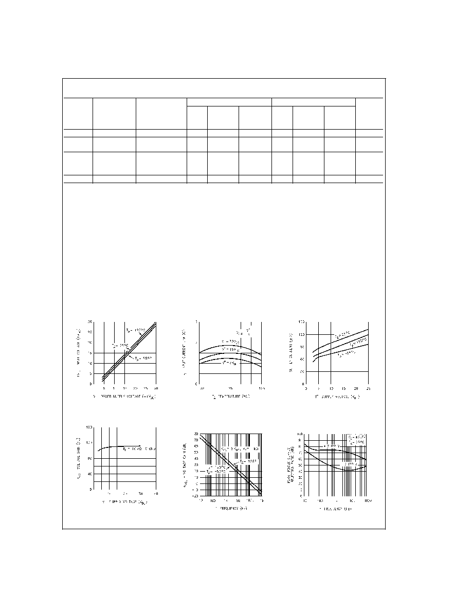
Typical Performance Curves
Input Voltage Range
DS008562-21
Input Current
DS008562-22
Supply Current
DS008562-23
Voltage Gain
DS008562-24
Open Loop
Frequency Response
DS008562-25
Power Supply
Rejection Ratio
DS008562-26
www.national.com
3
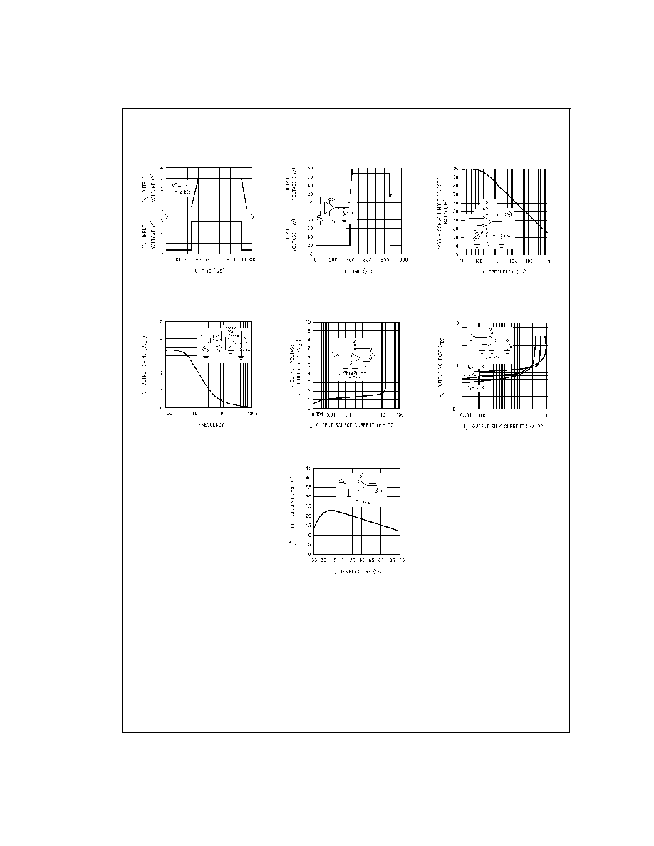
Typical Performance Curves
(Continued)
Application Hints
The LP324 series is a micro-power pin-for-pin equivalent to
the LM324 op amps. Power supply current, input bias cur-
rent, and input offset current have all been reduced by a fac-
tor of 10 over the LM324. Like its predecessor, the LP324 se-
ries
op
amps
can
operate
on
single
supply,
have
true-differential inputs, and remain in the linear mode with an
input common-mode voltage of 0 V
DC
.
The pinouts of the package have been designed to simplify
PC board layouts. Inverting inputs are adjacent to outputs for
all of the amplifiers and the outputs have also been placed at
the corners of the package (pins 1, 7, 8, and 14).
Precautions should be taken to insure that the power supply
for the integrated circuit never becomes reversed in polarity
or the unit is not inadvertently installed backwards in the test
socket as an unlimited current surge through the resulting
forward diode within the IC could destroy the unit.
Large differential input voltages can be easily accommo-
dated and, as input differential voltage protection diodes are
not needed, no large input currents result from large differen-
tial input voltages. The differential input voltage may be
larger than V
+
without damaging the device. Protection
should be provided to prevent the input voltages from going
negative more than -0.3 V
DC
(at 25∞C). An input clamp diode
with a resistor to the IC input terminal can be used.
Voltage Follower
Pulse Response
DS008562-27
Voltage Follower Pulse
Response (Small Signal)
DS008562-28
Common Mode
Rejection Ratio
DS008562-29
Large Signal
Frequency Response
DS008562-30
Output Characteristics
Current Sourcing
DS008562-31
Output Characteristics
Current Sinking
DS008562-32
Current Limiting
DS008562-33
www.national.com
4
Application Hints
(Continued)
The amplifiers have a class B output stage which allows the
amplifiers to both source and sink output currents. In appli-
cations where crossover distortion is undesirable, a resistor
should be used from the output of the amplifier to ground.
The resistor biases the output into class A operation.
The LP324 has improved stability margin for driving capaci-
tive loads. No special precautions are needed to drive loads
in the 50 pF to 1000 pF range. It should be noted however
that since the power supply current has been reduced by a
factor of 10, so also has the slew rate and gain bandwidth
product. This reduction can cause reduced performance in
AC applications where the LM324 is being replaced by an
LP324. Such situations usually occur when the LM324 has
been operated near its power bandwidth.
Output short circuits either to ground or to the positive power
supply should be of short time duration. Units can be de-
stroyed, not as a result of the short circuit current causing
metal fusing, but rather due to the large increase in IC chip
dissipation which will cause eventual failure due to exces-
sive junction temperatures. For example: If all four amplifiers
were simultaneously shorted to ground on a 10V supply the
junction temperature would rise by 110∞C.
Exceeding the negative common-mode limit on either input
will cause a reversal of phase to the output and force the am-
plifier to the corresponding high or low state. Exceeding the
negative common-mode limit on both inputs will force the
amplifier output to a high state. Exceeding the positive
common-mode limit on a single input will not change the
phase of the output. However, if both inputs exceed the limit,
the output of the amplifier will be forced to a low state. In nei-
ther case does a latch occur since returning the input within
the common mode range puts the input stage and thus the
amplifier in a normal operating mode.
The circuits presented in the section on typical applications
emphasize operation on only a single power supply voltage.
If complementary power supplies are available, all of the
standard op amp circuits can be used. In general, introduc-
ing a pseudo-ground (a bias voltage reference to V
+
/2) will
allow operation above and below this value in single power
supply systems. Many application circuits are shown which
take advantage of the wide input common-mode voltage
range which includes ground. In most cases, input biasing is
not required and input voltages which range to ground can
easily be accommodated.
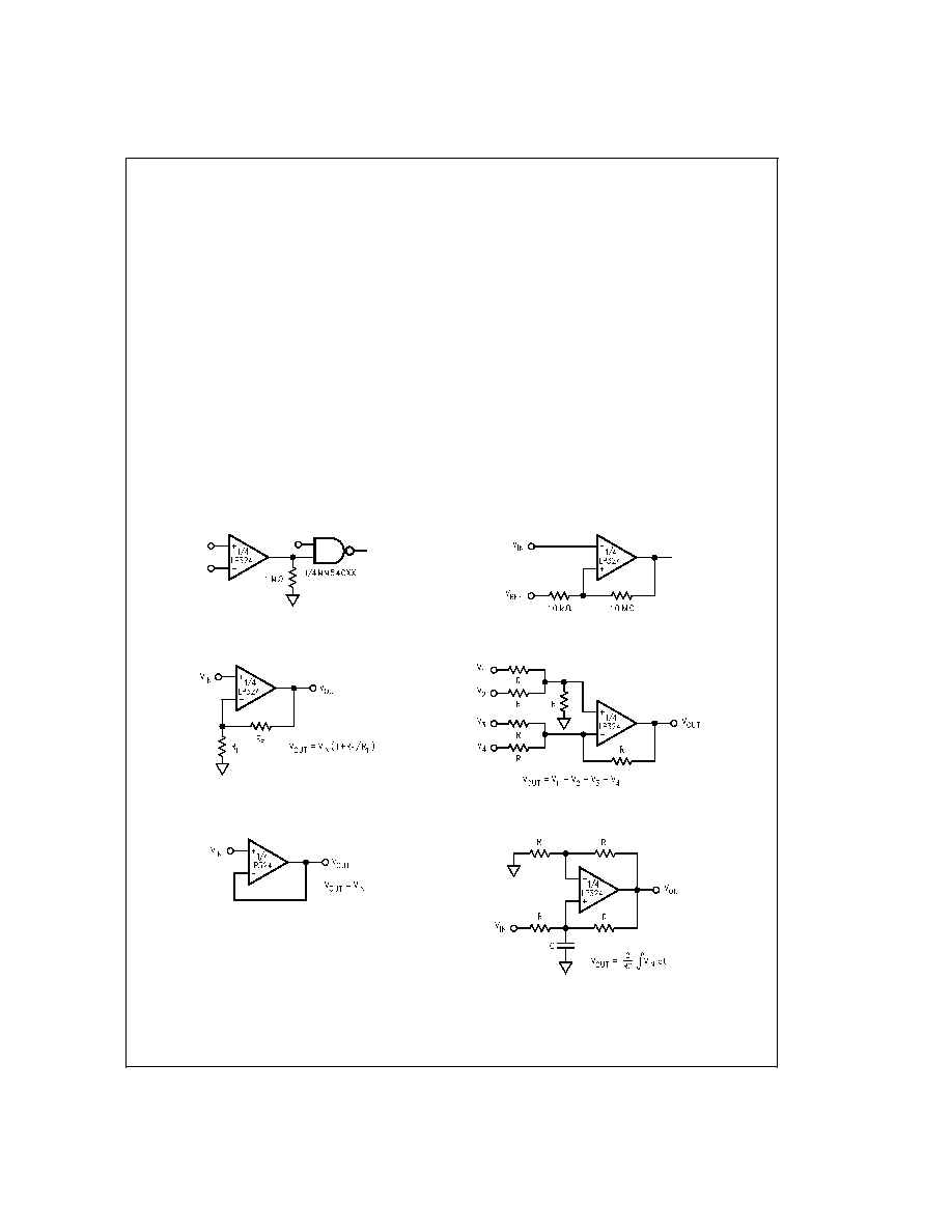
Driving CMOS
DS008562-3
Comparator with Hysteresis
DS008562-6
Non-Inverting Amplifier
DS008562-4
Adder/Subtractor
DS008562-7
Unity Gain Buffer
DS008562-5
Positive Integrator
DS008562-8
www.national.com
5
Application Hints
(Continued)
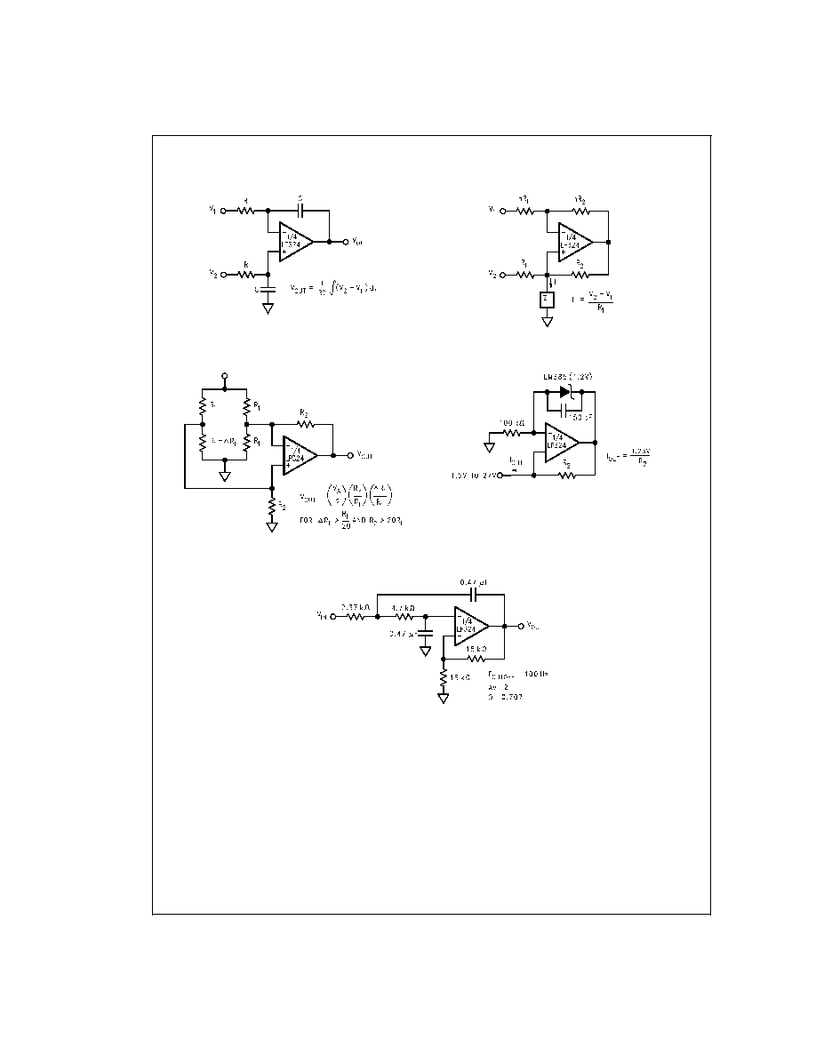
Differential Integrator
DS008562-9
Howland Current Pump
DS008562-10
Bridge Current Amplifier
DS008562-11
µ Power Current Source
DS008562-12
Lowpass Filter
DS008562-13
www.national.com
6
Application Hints
(Continued)
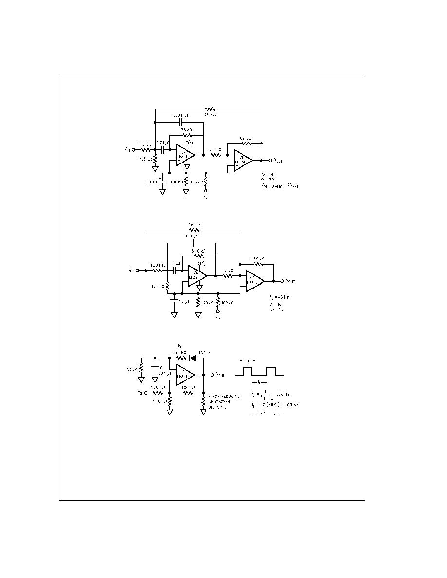
1 kHz Bandpass Active Filter
DS008562-14
Band-Reject Filter
DS008562-15
Pulse Generator
DS008562-16
www.national.com
7
Application Hints
(Continued)
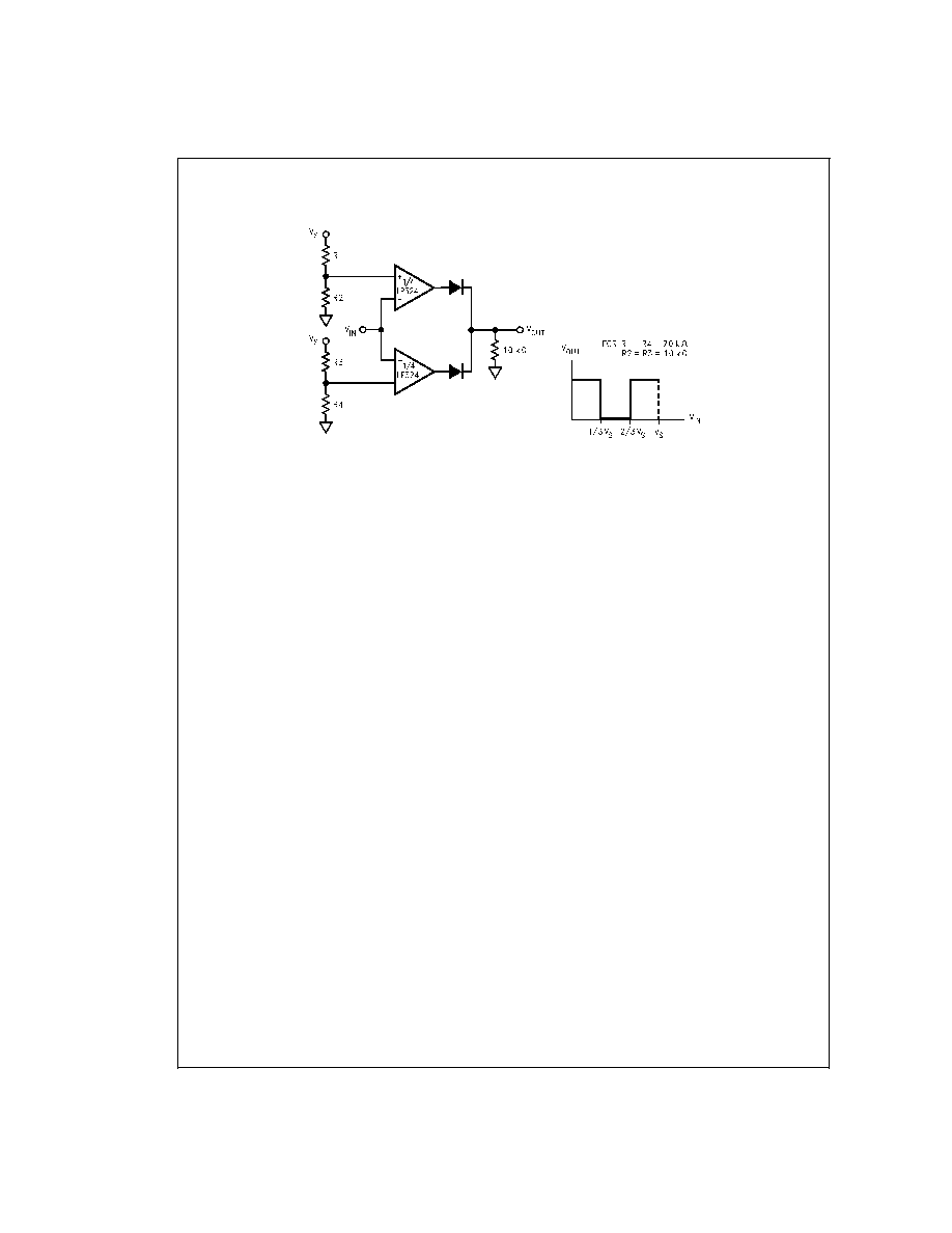
Window Comparator
DS008562-17
www.national.com
8
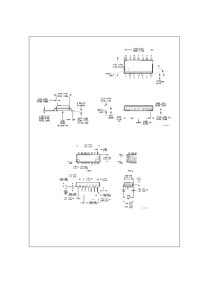
Physical Dimensions
inches (millimeters) unless otherwise noted
S.O. Package (M)
Order Number LP324M or LP2902M
NS Package Number M14A
Dual-in-Line Package (N)
Order Number LP324N or LP2902N
NS Package Number N14A
www.national.com
9

Notes
LIFE SUPPORT POLICY
NATIONAL'S PRODUCTS ARE NOT AUTHORIZED FOR USE AS CRITICAL COMPONENTS IN LIFE SUPPORT
DEVICES OR SYSTEMS WITHOUT THE EXPRESS WRITTEN APPROVAL OF THE PRESIDENT AND GENERAL
COUNSEL OF NATIONAL SEMICONDUCTOR CORPORATION. As used herein:
1. Life support devices or systems are devices or
systems which, (a) are intended for surgical implant
into the body, or (b) support or sustain life, and
whose failure to perform when properly used in
accordance with instructions for use provided in the
labeling, can be reasonably expected to result in a
significant injury to the user.
2. A critical component is any component of a life
support device or system whose failure to perform
can be reasonably expected to cause the failure of
the life support device or system, or to affect its
safety or effectiveness.
National Semiconductor
Corporation
Americas
Tel: 1-800-272-9959
Fax: 1-800-737-7018
Email: support@nsc.com
National Semiconductor
Europe
Fax: +49 (0) 1 80-530 85 86
Email: europe.support@nsc.com
Deutsch Tel: +49 (0) 1 80-530 85 85
English
Tel: +49 (0) 1 80-532 78 32
FranÁais Tel: +49 (0) 1 80-532 93 58
Italiano
Tel: +49 (0) 1 80-534 16 80
National Semiconductor
Asia Pacific Customer
Response Group
Tel: 65-2544466
Fax: 65-2504466
Email: sea.support@nsc.com
National Semiconductor
Japan Ltd.
Tel: 81-3-5639-7560
Fax: 81-3-5639-7507
www.national.com
LP2902/LP324
Micropower
Quad
Operational
Amplifier
National does not assume any responsibility for use of any circuitry described, no circuit patent licenses are implied and National reserves the right at any time without notice to change said circuitry and specifications.